Exhibit 99.3

| The next generation of wafer stages Frank van de Mast and Harry van der Schoot 15 October 2008, Veldhoven |

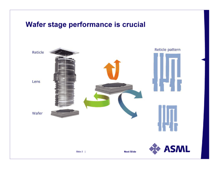
| WAFER Next Slide Wafer stage performance is crucial Wafer stage performance is crucial |

| Higher throughput due to faster acceleration time speed a - a ^t t a - a t TWINSCAN XT TWINSCAN NXT speed time |

| ASML wafer stage drivers Productivity - speed/acceleration - performance wafer stage Initial throughput improvement of more than 30% Overlay - accuracy - measurement system New measurement system to position wafer more accurately overlay improvement by 50% Resolution - Focus point Lens Shrink improvement by 42% with double patterning |

| Performance |

| Advanced materials and compact design results in total weight reduction of 66% ? Faster acceleration |

| NXT Wafer Stage Improves Throughput and Overlay Goal Design Reduce Exposure Time Higher Acceleration Light-Weight Construction Reduce Exposure Time Higher Acceleration New Actuators for high force Reduce Overhead Very Fast Chuck Swap Autonomous chucks during swap Reduce Overhead Seamless Immersion Swap Swap under Lens Improve Overlay Accurate Position Measurement Grid Plate Measurement System Improve Overlay Robustness for Disturbances Grid Plate Measurement System |

| sequential operation Parallel operation reduced time needed per wafer Productivity increase Time needed to expose a single 300 mm wafer ^ scan time step time wafer load + global + fine align metrology operation parallel operation wafer exposure operation scan time wafer measurement + align step time swap no overhead operation wafer exposure operation metrology operation wafer map + align scan time step time swap increase of througput maximize measurement time increase of througput maximize measurement time |

| stage swap stage swap stage swap Performance: 'Journey of a wafer' on dual wafer stages align reticle expose position measurement position align wafer expose wafer load wafer unload wafer measure wafer |

| Accuracy |

| What does overlay mean? Overlay up to 2 nanometers 1 nm = 4 silicon atoms |

| Wafer stage metrology impact on overlay Inter- ferometer 300 mm stage Current stage metrology X-coordinate Y- coordinate Overlay [nm, 99.7%] Overlay: < 2 nm Wafer [#] (prototype) 0 2 4 6 8 10 1 2 3 4 5 6 7 8 9 10 11 Overlay: < 4 nm System [#] (ArF 0.93NA) 0 2 4 6 8 10 1 2 3 4 5 6 7 8 9 10 11 Overlay [nm, 99.7%] Inter- ferometer 300 mm stage Current stage metrology <15 mm stage Grid plate Improved metrology |

| Conclusion The NXT TWINSCAN platform offers opportunities to significantly improve overlay and productivity. Overlay The new wafer stage is suitable for double patterning techniques which manufacturers need for 32 nm node and beyond. Productivity The platform makes it possible to continue the semiconductor industry's roadmap for more advanced and affordable chips. |